List of all Early Stage Researchers
Name : Ratish Rao
Associated to : University of Lyon – Laboratoire Hubert Curien
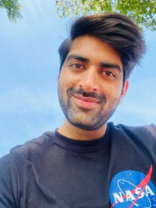
About me : My name is Ratish Rao. I am an Indian. I did my bachelors in electronics and communication engineering in Bangalore. I was intrigued by optics during my engineering days and I wanted to know more about light. Hence, I studied masters in photonics at University of Eastern Finland. My growing interest towards integrated photonics prompted me to work with Multi-Mode Interferometers on low refractive index contrast waveguide platform as my master’s project. I was keen on taking my research interest forward and came across GREAT program which matched my idea of developing nanophotonic devices for industrial applications. As ESR-2 at LabHC, France, my work objective will be to design, fabricate and characterize GWS for spectral stabilization and wavelength multiplexing of high-power lasers in wide wavelength range. I believe that being part of GREAT ETN will greatly facilitate my understanding of design, fabrication and characterization department in photonic device production. I look forward to work and collaborate with other research groups and industrial partners in the consortium, which will help me succeed as a researcher in the field of integrated photonics.
Name : Giovanna Capraro
Associated to : AMO GmbH
About me: I am Giovanna, I come from a small coastal town in Apulia, Italy and I studied for both my Bachelor’s and Master’s degree in Physics at the University of Pisa. Since the beginning of my studies I have been interested in a wide variety of fields, such as condensed matter physics, photonics and optics. During my Master’s thesis work, in fact, I studied the properties of graphene in FETs, focusing on photonic devices fabrication and characterization.
My interest in this kind of work has been growing ever since, but I also wanted to expand my area of expertise into the field of optics: this is why the GREAT project fits this goal perfectly, in addition to cover such a fascinating topic as GWS. Moreover, it will give me the opportunity to collaborate with other researchers and industrial partners in a stimulating international environment, which will surely enrich me as a scientist. At AMO GmbH, Aachen, I will focus on developing and optimizing new methods to fabricate and characterize GWS, which will be implemented in laser systems for pulse compression.
Associated to : University of Eastern Finland – Department of Physics and Mathematics
About me : I was born in Siberia (Russia), graduated from St.Petersburg Polytechnic University and became a Master in Technical Physics. I worked at St. Petersburg Academic University in Nanophotonics laboratory and was involved in measurements of semiconductor structures by means of confocal microscopy, atomic-force microscopy and near-field scanning optical microscopy. And then the destiny gave me a chance to gain experience in the University of Eastern Finland. I am lucky to be a part of this GREAT project as Early Stage Researcher 4. It is so exciting to go through the whole process from design of structures and development to their application. I am working at UEF doing nanofabrication during this project. I can’t express how happy I am to be in Finland and have experienced and patient colleagues. Looking forward to gaining experience with my colleagues and collaborating within these 3 years!
Name : Fangfang Li
Associated to : University of Eastern Finland – Department of Physics and Mathematics
About me : I come from a small village in the center of China. I completed my bachelor’s and master’s degree studies in optical engineering at Beijing Institute of Technology. I have been studying optics since my undergraduate study. During my master’s study, I have been focusing on micro and nano-optics and have gained rich experience in grating design.
I took a glimpse of the advanced nanofabrication methods and was attracted by theses fascinating methods. Being equipped with basic knowledge and design skills is not enough for me to pursue my career. I am eager to fully understand the whole process of nanotechnologies from principle to design, to fabrication, to characterization, and then to implementation. It would help me to develop expertise and lay a solid foundation for my future career. Therefore, I was excited when I saw this PhD training opportunity provided by the GREAT project.
Thus, I joined the GREAT project as ESR-5 in University of Eastern Finland right after I got my master’s degree without hesitation. My main job is working on the fabrication of GWS for radial and azimuthal polarization shaping in high-power lasers for both intra-cavity and extra-cavity conditions. I am really honored to have this opportunity to work collaboratively with other researchers and partners and to contribute to this research activity.
Janis Zideluns
Associated to : Ecole Centrale Marseille – Institut Fresnel
About me: My name is Janis, I come from Latvia. There I received both my bachelors and Masters degrees from University of Latvia, faculty of Physics, Mathematics and Optometry. In parallel to my masters studies I started to work in the R&D team at the company SIA Groglass. During my time there I gained experience and knowledge about thin film deposition using magnetron sputtering. It was challenging and interesting work, so to further enhance my carrier I decided to look for PhD opportunities. My role in GREAT will be to fabricate thin film structures. In order to achieve that I will explore various methods of thin film monitoring learn to operate Buhler HELIOS coater and develop strategies of thin film optical monitoring. During my PhD I will collaborate with industrial partners and other research groups.
Associated to : University of Southampton – Optoelectronics Research Centre
About me : After high school, I studied general physics and mathematics for two years and took competitive exams to enter a French “Grande Ecole”. As a result, I was accepted in Institut d’Optique Graduate School in 2015 and started studying the basics of photonics. Little by little, I realised that this field was extremely vast and very exciting. I completed my studies with a MSc Optics and Photonics at Imperial College London. My Master’s thesis aimed at spreading the hollow fibre pulse compression method by overcoming its main weakness : the sensitivity to the alignment.
Three years of theoretical and practical knowledge in photonics were not enough to satisfy me : I wanted to further develop my research skills with a PhD. The GREAT consortium gives me the opportunity to work within an international context and with a strong industrial perspective. My role in the network is to improve crystalline thin film growth methods, which could give better thermal and mechanical properties to our grating waveguide structures.
Associated to : University of Stuttgart – ITO
About me : My name is Anton Savchenko and I am from Russia. I graduated from ITMO University as an engineer in optoelectronic devices and systems several years ago. After that I worked as a mechanical engineer designing and building different devices such as gas detectors and stretch film rewinding machines. In 2018 I was admitted to the master’s program in photonics at University of Eastern Finland and I graduated with a thesis focused on the integration of a LED-based tunable light source to a mini-endoscopic system in 2020. I joined the GREAT project as ESR-8 at ITO because this project provides a unique opportunity to gain and develop expertise in photonics and microfabrication as well as chance to collaborate with fellow researchers across Europe. I will work on the fabrication of circular and segmented grating-waveguide structures using scanning beam interference lithography (SBIL) and stepped mask interference lithography (SMILE). I am honored to be a part of GREAT project.
Name : Georgia Mourkioti
Associated to : University of Southampton – Optoelectronics Research Centre
About me : My name is Georgia Mourkioti and I am from Greece. I received my BSc degree in Materials Science in 2016 from the University of Patras, Greece and my MSc in Materials Science in 2019, from the same University. My undergraduate thesis was on the design of photonic structures for applications in optical memory media and it was a collaboration with a company in Greece named ‘OPTICON GROUP ABEE’. My master thesis was on the study of slow light and polarization dynamics in quantum-dot vertical-cavity semiconductor structures. During my postgraduate studies I was awarded the ‘’K. KARATHEODORI’’ scholarship from the University of Patras, Greece and I have co-authored 2 journal and conference publications:
1) Mourkioti, G., et al. « Slow light in quantum dot vertical cavity semiconductor optical amplifiers. » Semiconductor Science and Technology 34.6 (2019): 064004.
2) Georgiou, Panagiotis, Georgia Mourkioti, and Dimitris Alexandropoulos. « Impact of the Excited State on the Dynamics of Spin-Polarized Quantum-Dot Vertical Cavity Surface Emitting Lasers. » 2019 Conference on Lasers and Electro-Optics Europe & European Quantum Electronics Conference (CLEO/Europe-EQEC). IEEE, 2019.
By the end of my studies I was convinced that Photonics was a passion for me. So, I’d started seeking for my future research steps in this field when I stumbled on GREAT project. And the journey began. I am ESR-9 at ORC/Zepler Institute in the University of Southampton. My objective will be to develop processes to create sub-wavelength structures in crystalline materials, both in substrates and in films fabricated by Pulsed Laser Deposition (PLD), including crystalline mirrors and waveguide structures. Through the project GREAT I will have the opportunity to gain high standards of knowledge in the field of Photonics, as well as to collaborate with excellent research and industrial partners.
Marek Stehlík
Associated to : Ecole Centrale Marseille – Institut Fresnel
About me : I am Marek Stehlík and I come from the Czech Republic. I am a Master´s degree graduate in Laser Technology and Electronics at the CTU in Prague. In my Master´s thesis, I dealt with tunable ytterbium lasers. I studied wavelength selectivity and output characteristics with different dispersive prisms and birefringent filters. However, it is the diffraction grating that attract my attention in terms of spectral stability, broad wavelength tunability, effective pulse-compression or possibility to be implemented in laser systems generating high-energy ultra-short pulses. After graduation I spent two inspiring years at HiLASE centre, technological institute aiming to the development of high-power laser systems. Thanks to my work on material damage resistance via fs and ps pulses, I have come to realize that the critical parameter of the high-power systems is laser-induced damage threshold of optical components. Therefore, I see the mission of ESR-10, study of laser damage resistance of materials and structures for grating-waveguide, as very perspective for the development of industrial lasers. I am very thankful that as ESR-10 working at Fresnel Institute in Marseille I can be a part of the GREAT innovative training programme.
Associated to : Alphanov – Laser sources and components
About me : My name is Adrian Grande and I come from Spain where I studied my bachelor in Engineering Physics at Universitat Politècnica de Catalunya (UPC) in Barcelona. I have always been interested in photonics due to the unique properties of light finding applications in many fields, that is why I studied an Msc in Optics and Photonics at Imperial College of London. During my Msc thesis, I designed, modelled and built an optical levitation trap with the largest trapping distance reported so far suitable for high power laser experiments in vacuum. I am so lucky to be part of the GREAT project as Early Stage Researcher 11. I am working at Alphanov and my main duties are the development of mid-IR laser sources and laser technologies such as amplifiers and CPA architectures for advanced scientific applications and to demonstrate the potential of highly efficient compressors developed within the GREAT project. I am looking forward to gain expertise in the field of photonics and to meet and collaborate with my colleagues.
Name: Denys Didychenko
Associated to: University of Stuttgart – IFSW
About me: Born in Kyiv, Ukraine. Got my degree in Electronics at Kyiv Polytechnic Institute. My practical experience there was related to solar cells. During my Masters in Ukraine I was looking for a mobility opportunities to develop my skills in engineering. As a result I was in enrolled as double degree student at Korea Institute of Science and Technology, where my laser life started. For two years in Korea I was dealing with mode-locked fiber lasers. At this time I was thinking about further opportunities in laser industry and one of the project that interested me a lot was the GREAT. In the spring 2020, I was close to get my Master in Korea and I started to look for a place to do my PhD. What was my surprise when I found GRAET again with opened position. I believe it was sign for me, so I applied and was approved as ESR 13. Now, I am working in University of Stuttgart working on generation of radially and azimuthally polarized beams in thin-disk laser . I believe that my colleagues and I will be able to achieve results that will introduce valuable impact in science.
Associated to : University of Bordeaux – Laboratoire Ondes et Matiere d’Aquitaine
About me: My name is Muhammad Ghawas. I am from Pakistan. Due to my immense interest in the field of photonics, I opted “Lasers and optoelectronics” as my major in my bachelor’s degree. Afterward, I did master’s in “Photonics” at the University of Eastern Finland (UEF) and graduated in 2020. During my master’s degree, I have worked on a thesis project focusing on the development of an ultrafast mode-locked laser with a few GHz pulse repetition rate at VTT MIKES (Center for Metrology), Finland. To continue working in the field of lasers and gain an in-depth understanding of the subject, I have started a Ph.D. within the GREAT project as an Early-Stage Researcher (ESR-14) at Laboratoire Ondes et Matiere d’Aquitaine (LOMA), University of Bordeaux. I am currently working on the development of high-power picoseconds/femtoseconds Ytterbium (Yt3+) fiber laser sources for the applications of the optical parametric oscillator (OPO) and amplification (OPA). In this work, my goal is to implement Grating waveguide structures (GWS) within the laser cavity for spectral stabilization and spectral width tunability. I am so privileged to be a part of a GREAT team and I look forward to having an amazing experience.
Name : Sayed Muhammad Baker
Associated to : DILAS Diodenlaser GmbH – Beam sources department
About me: My name is Sayed Muhammad Baker. I come from the capital city named “Dhaka” from Bangladesh.
Optics and LASER technology have made a revolutionary impact on the world. The challenges and scopes of learning new things in this field are irresistible. To me this field is extremely appealing, as researchers in this field work at the forefront of technology. Not only are they expanding the horizon of science but also constantly pushing technology to its ultimate limits.
I completed my undergraduate studies in the domain of Electrical and Electronic Engineering. I found that the knowledge I gained, is only the tip of an iceberg and to be a specialist in basic electronics of my field of interest, I have to go a long way through the path of higher studies on Optics and LASER technology. Being oriented in that direction, I completed my first Master’s Program in the field of Optics. My thesis was focused on Laser Technology and the successfully completed thesis topic was “Optimization and Improvement on the Performance Characteristics of a 450 nm True Blue Edge Emitting Laser” where I became acquainted with the properties, applications and knowledge of LASER technology and Optics.
To become more eligible for an international program like GREAT, I enrolled myself to the second Master’s program (MSc) in “Molecular Nano and BioPhotonics for Telecommunications and Biotechnologies (MONABIPHOT)” among the prestigious European Union’s Erasmus Mundus graduate programs. This second graduate program has introduced me to the methodology of research in the fields of LASER technology and Optics with the state-of-art technology. I completed my MONABIPHOT Master’s thesis on “Development of a Femtosecond Neodymium Doped Fiber Based Laser for Neuroscience Applications” at Charles Fabry Laboratory of Institut d’Optique in Paris, which allowed me to concentrate all my attention to the area of my interest.
Currently I am employed as a project Engineer at « COHERENT-DILAS Diodenlaser GmbH » for the MSCA-ITN-ETN project GREAT (ESR 15). My research goal is (i) to investigate the specification and performance of different Grating Waveguide Structures and comparing to existing Volume Bragg Gratings and (ii) to investigate different Grating Waveguide Structures for accomplishing efficient wavelength coupling of diode modules. I recognize the fact that the project beneficiaries and partners are a remarkably strong and an attractive place to embark on a research career. Being oriented in this direction for a long period, I am confident of contributing significantly in this field with the continuous collaboration with outstanding supervisors and the other Early Stage Researchers.
Former members
Haidi Haytham
About me : My name is Haidi Haytham Badawi. I am from Egypt. I got my BSc degree in Mechatronics Engineering from the German University in Cairo in 2015. I conducted my bachelor thesis in the DHBW Stuttgart. The objective of my bachelor’s thesis was the design of selective surfaces to study their effect on electronics cooling using finite element analysis. This project was a collaboration with Robert Bosch. Later in 2019, I received my master’s degree from the same university. The objective of my master’s thesis was to design an optomechanical frequency analyzer using micro-optical dielectric resonators based on Whispering Gallery Modes (WGM). During my postgraduate studies, I was co-authored in one journal in JOSA B and one conference paper in SPIE 2018. After finishing my master’s degree I wanted to further explore the field of photonics and develop my research skills. Therefore, I decided to pursue my doctoral studies and started to search for available positions in this field until I had the opportunity to join the GREAT project. My role in the project is the fabrication of the grating waveguide structures for large areas using scanning beam and stepped mask interference lithography (SBIL & SMILE) to be used for high power laser applications.
Lukas Müller
About me: My name is Lukas and I am from Germany. I studied at the University of Stuttgart, where I received my B.Sc. degree in Physics in 2015 and in 2017 my M.Sc. degree in Photonic Engineering.
My master’s thesis was focused on the characterization of Grating waveguide structures similar to those which shall be developed and produced within the Great project. After that I collected some experience in the development of pulsed laser systems based on the thin-disk technology in the company Dausinger+Giesen GmbH in Germany. To deepen my knowledge in the field of lasers and laser optics I decided to apply for a Ph.D. within the GREAT project.
My task in this project is to verify and test the ability of the developed gratings to be used in state-of-the-art laser systems. Therefore I want to make use of the wavelength-selectivity to create a spectral filter for the setup of a high-power, modelocked Yb-fiber laser system as well as to use them to compress the output pulses.

